By Joe Aguilar, Senior Manager, Principal Engineer
In this overview of the principles of high-performance PCB layout, Joe Aguilar illustrates thermal design approaches, supplies a synopsis of the power delivery network (PDN), tells strategies for routing high currents with reduced impedance, and provides important considerations for designing effective decoupling capacitance.
Power design for high-performance computing: The mission-critical PCB
Power system design tends usually to focus on converters, discrete components, and accessories required to get power from the source to the load – treating the printed circuit board (PCB) as a mounting and routing plane and relying primarily on feedback and control circuits to compensate for the many small losses and impedances in a typical PCB. In recent years, however, high-density loads like processors for artificial intelligence (AI) and supercomputing have become more sophisticated and much faster, pushing every component to perform at maximum capability.
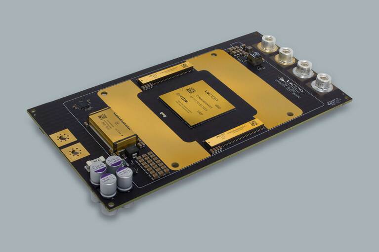
Exacting voltage-regulation requirements and extremely high transient slew rates mean that every source of voltage drop and every source of power loss within the system, no matter how small, has a measurable negative impact. PCB layout is therefore critical to achieving high-performance power. This brief overview of the principles of high-performance PCB layout includes thermal design approaches, an overview of the power delivery network (PDN), strategies for routing high currents with reduced impedance, and some important considerations for designing effective decoupling capacitance. Figure 1 shows a design created by Vicor for testing and demonstration that will be used in this article.
Figure 1: In this test board from Vicor, a PRM™ regulator and two VTM™ current multipliers mounted on a high-density PCB supply power to a load module that simulates a high-performance computing processor. In operation, a cold plate or heat sink would be mounted over the VTMs and load module, and another heat sink would be mounted on the PRM.
Thermal design
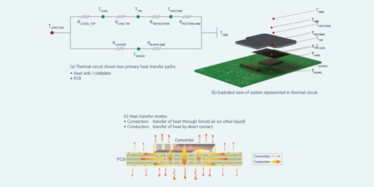
The goal of thermal management in electrical power system design is to move heat efficiently from heat-producing junctions to the ambient air. Some transfer will occur naturally, but even in conventional designs it is usually necessary to add heat sinks and fans. A detailed analysis of heat transfer with a focus on the PCB early in the design process is required for high-density systems in order to make maximum use of the PCB itself as a conductor of heat.
Figure 2: Conduction to and through the PCB is an important part of high-density thermal management, and requires the use of equivalent circuits to determine the most effective thermal paths (a), (b). Good thermal design optimizes both conduction and convection heat transfer modes (c).
The primary sources of heat in an electrical power system are the internal junctions of active components like power converters. Though for the purposes of a topological thermal model they can be represented as a node at one end of an equivalent circuit (see Figure 2(a)). Each component or material that the heat from that internal junction must pass through in order to reach the ambient air surrounding the power system can be represented as a resistor impeding the flow of heat toward the ambient air. An equivalent thermal circuit shows the most obvious path heat follows from the internal junction of a power converter: through the case, thermal interface material (TIM) and finally heat sink to the ambient air. It also shows a second, less-obvious parallel path through the PCB. This second path is often overlooked, but it is hard to overstate its importance for high-density power design.
Thermal models can become fairly complex with a different thermal impedance for each net or land. Regardless of complexity, the thermal model will identify the nets with the lowest-impedance paths for carrying heat away from the internal junctions of a component. The designer can then use this information to maximize heat conduction by increasing copper dedicated to that net, i.e., extending external copper planes and using thermal vias to increase surface area beyond the minimum to increase heat-sinking potential. Various types of vias can be used where appropriate: stacked and buried vias, VIPPOs and traditional through-hole vias are all effective options in the designer’s tool kit.
PDN overview
PDN impedance, specifically within the PCB, is the area of critical focus for high-density computing power systems. These systems operate at extremely high frequency. In a typical high-performance computing power system, the PDN is made up of several elements between the output of the voltage regulator and the sense point, which is usually located inside the CPU either on the die or the ball grid array (BGA) interconnect. Bypass capacitors, decoupling capacitors with associated vias and BGA interconnect make up the discrete components of the PDN. The high-frequency load steps generated by powerful supercomputing processors are so fast that there's very little that the control loop can do to minimize the effects of the PDN. That's why the PDN is such an integral part of the design.
Figure 3: Impedances in the discrete components of the PDN between a voltage regulator and the CPU load, particularly at high frequencies and large load steps, can seriously impact the effectiveness of a power design.
High-current routing: Reducing PDN impedance
It's critical to define the PCB stackup and floor plan up front, including overall layer count, the number of layers dedicated to power and ground, and what copper weight to use. Next, identify dedicated layers for routing signals continuous ground planes. Then, define the layers needed for any nets that require impedance-controlled routing, have parasitic limits or bring other special considerations. Getting this right is crucial when designing for high-current processors drawing 1000 amps or more.
Some estimation techniques will speed up the early stages of PCB design, making it easier to employ simulation to refine the design still further. The squares method of estimating the copper plane resistivity is one simple and effective technique. A variation on the squares method can also be used for estimating the inductance of adjacent power and return planes.
Figure 4: The squares methods of estimating power plane resistance and inductance.
Via resistance and inductance can also be estimated with simple geometry-based calculations, because a via can be conceptualized as a thin sheet of copper rolled into a tube. Via resistance (R) is therefore equal to the product of the plating resistivity (r) and via length (L) divided by the plating cross-sectional area (A).
Figure 5: Via resistance can be estimated with simple geometry-based rules-of-thumb.
Parasitic capacitance is another significant source of impedance in a PCB, and it is therefore necessary to include in any simulation. As with the estimations of resistance and inductance, approximate calculation of the parasitic capacitance in a PCB starts from basic physical properties; in general, capacitance between a pair of parallel conductor planes increases proportionally with surface area; it also increases inversely with dielectric spacing.
Decoupling capacitance
High-density power systems require carefully selected decoupling capacitors to filter high-frequency switching noise. This sort of application requires capacitors exhibiting very low equivalent series resistance (ESR) and an appropriately high self-resonant frequency — beyond this point, a capacitor stops being an effective filter of high-frequency noise because its impedance becomes inductive due to equivalent series inductance (ESL). The capacitance value can be less important overall, even.
Figure 7: Capacitor selection and via placement are critical for achieving low-impedance filtering of high-frequency switching noise.
Achieving the low ESR and low ESL is the first object, and for this a designer should consider smaller low-inductance and reverse-geometry capacitors that place the positive and negative terminals closer together and increase the self-resonant frequency. Careful placement of both the component and the vias is important to minimize loop inductance.
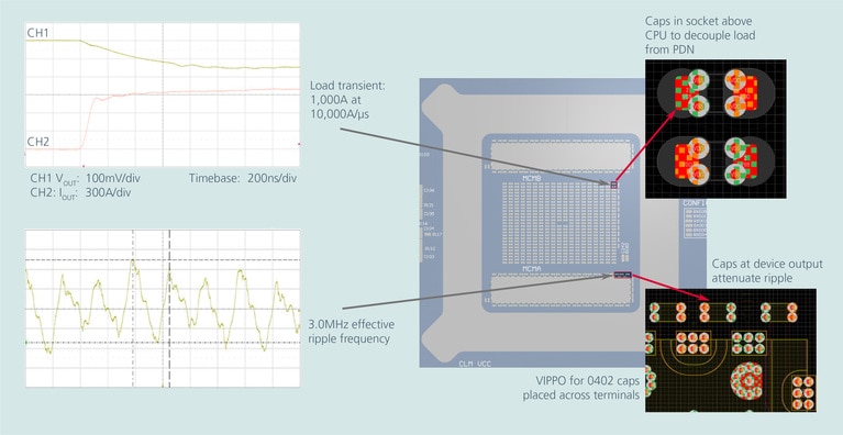
An example of a system designed to handle a 1000A load step at 10,000A/µs shows how 0402 decoupling capacitors placed very close to the power module attenuate ripple, while other capacitors in the socket decouple the load from the PDN.
Figure 8: Appropriate capacitor selection and placement using high-performing via arrangement makes 1000A load steps at 10,000A/µs possible.
Designing PDNs for high-performance computing and AI is a complex challenge, given the ever-increasing power requirements in terms of current levels and voltage accuracy required by today’s advanced processors. Up-to-date modeling and estimation techniques for thermal and PDN design, as well as advanced component selection and placement criteria are therefore required.
A more in-depth treatment of this topic is available in the Vicor on-demand webinar, High-performance PCB layout and thermal design techniques.
Joseph Aguilar is a Senior Manager of DC-DC Product Applications at Vicor. He has over 15 years of experience in the power electronics industry as an Applications Engineer. During his career, Mr. Aguilar has worked on products and applications in a wide range of areas including defense, industrial, telecom, lighting and computing. In his recent works, Mr. Aguilar has primarily focused on development of products and reference designs for high performance computing applications. Mr. Aguilar holds a BSEE in Electrical Engineering from Western New England College in Springfield Massachusetts.
Joe Aguilar, Senior Manager, Principal Engineer