

優化 DC-DC 轉換器穩定性:源阻抗效應的 AC 與瞬態模擬分析
探討如何通過頻域 AC 小訊號分析和時域瞬態分析來優化 DC‑DC 轉換器的穩定性
作者:David Berry,首席應用工程師
任務關鍵型、快速啟動隔離電源系統的設計必須完美無缺。 這些系統需要在毫秒級時間內啟動,並且每次都必須成功啟動。
在電子系統中,電源的設計目的是為負載提供穩定的電壓和/或電流。 設計電源系統時,人們通常關注其對快速變化的負載以及負載所需快速變化電壓的響應能力。 而對電源系統的輸入電壓和啟動時間則關注較少,因為人們通常假設系統電源始終存在。
然而,有些系統中電源並非始終存在,並且系統必須在施加輸入電源後的數毫秒內啟動。 這些系統通常需要與電源隔離,以保持接地隔離或滿足軍用規範,例如軍標 MIL-STD-704。
例如,在許多導彈發射系統中,目標資訊直到發射前一刻才被程式設計到飛彈中。 在目標資訊加載之前,飛彈內部有多個系統需要啟動,而電源系統只是其中之一,並且它需要第一個被啟動,以驅動所有其他系統。因此,正確設計電源系統至關重要。
在設計必須在輸入電壓施加後 10 毫秒內啟動的隔離電源系統時,有幾個關鍵領域需要考慮:輸入 dV/dt 不應超過電源組件的額定值; 輸入電容不應導致電源組件超出其額定值; 輸出電容值的選擇應確保系統不會進入電流限制狀態或表現出不穩定性。
許多 DC-DC 轉換器的輸入部分包含一個LC濾波器。 如果該 LC 濾波器受到階躍電壓衝擊(即向電源系統施加直流電壓),可能會產生振盪,導致電壓峰值升高至足以損壞電源組件內部電路的水准。 最大輸入 dV/dt 的常見限值是 10V/ms。 機械切換或閉合過快的 FET 很容易超過 10V/ms 的上升時間。 採用模組化電源方法,帶有限流功能的輸入濾波器可以將 DC-DC 轉換器的輸入保持在輸入 dV/dt 規格範圍內。
圖 1 顯示了電源系統框圖,圖2顯示了典型輸入濾波器內部結構框圖。 通常,穩壓 DC-DC 轉換器的輸入端需要一個輸入電容器,這是因為它需要呈現低源阻抗,並確保轉換器在輸入電壓和負載變化時保持工作穩定性。這個電容器需要緩慢充電,以避免超過最大 dV/dt,但又必須足够快,以幫助實現電源系統啟動時間小於 10 毫秒的設計目標。在系統輸入電壓施加之初,圖 2 中的 Q1 處於關斷狀態。 當電壓達到欠壓開啟閾值時,圖 2 中的電荷泵控制模組將開始推動 Q1,並升高濾波器的輸出電壓。 這一輸出電壓的上升過程受到精確控制,以確保其不超過轉換器的 dV/dt 限制,同時控制從電源端汲取的電流。

圖 1:電源系統框圖。

圖 2:典型輸入濾波器內部結構框圖。
To aid in achieving a less than 10ms start time, the filter must charge its output C as fast as possible. Selecting the lowest value of this output capacitor is best when designing for a fast turn-on time. Using an unregulated isolator at the output of the filter would be best because these require little to no input capacitance and because they don’t regulate, thus a control loop is unaffected. A good input filter will also include EMI and transient protection to meet Mil 461 standards for EMI and Mil 704 and Mil 1275 for input transients.
If an isolator is used at the output of the filter and the filter output rise time is controlled, then the output of the isolator will be controlled. The isolator’s output mirrors the input by the voltage ratio of the converter. This will keep the downstream regulators in Figure 1 within their input dV/dt specification range. The regulation stage does need input capacitance for source impedance requirements and stability. So this needs to be taken into account when determining capacitance seen by the filter. The isolator will reflect its output capacitance to its input and this will be seen by the input filter.
The capacitance reflection is the isolator’s output / input voltage ratio squared, multiplied by the isolator’s output capacitance. If the output / input voltage ratio is 1/2 and the isolator’s output capacitance is 47μF, then the reflected capacitance to the filter is 1/2 squared times 47μF or 11.75μF. The performance of the isolator is critical in this application. The isolator needs to have very little inductance as part of its power train. The low values for inductance allows current to flow rapidly from input to output while maintaining a fixed input to output voltage ratio. Some isolators have power train internal inductances in the nH range.
The input filter also keeps the source from exceeding its maximum current ratings. As an example, during a high dV/dt event such as a hot plug, mechanical switch or FET switch closing, the filter will shield any capacitance from seeing this high dV/dt. The power system source always has a maximum‑current rating due to source capability, connectors and traces that go to the power supply. If these components see higher-current levels they can fail or become weakened and turn into latent failures. In power systems that require less than 10ms start up, the input voltage to the supply must come up quickly as this timing is part of the 10ms start up. A quick start up into capacitance will result in high inrush current. The filter helps to reduce this inrush. Many filters have inrush ratings in amps per output μF. If the rating is 0.007A/μF and you have 47μF at the filter’s output, then the inrush current is 0.007A*47μF or 0.329A.
In many applications, the power supply will have its own output capacitance as well as load capacitance. This capacitance is charged by the output voltage of the converters. When designing for a less than 10ms start time, the output voltage rise across the output capacitance must not cause the converter to exceed its current maximum, resulting in shut down or output voltage dip due to current limit. If the converter shuts down and restarts, then the start-up time is lengthened. If the converter goes into current limit then the output voltage drops, resulting in a longer rise time and extension of the start-up period. Taking this into account, it is best to design using the smallest amount of output capacitance possible. The output current charging the output capacitance is determined by the equation:

I is the converter output current, C is the output capacitance and dV/dt is the converter output voltage rise time. If the load is active during the rise time then this needs to be added to the current supplied by the converter. In either case, the current should not exceed current maximum. If the current does exceed the maximum, then another converter in parallel can be added to boost the current rating of this output.
The output capacitance of the converter helps keep the converter output ripple low as well as help keep the converter stable during operation. Using a converter with a high-switching frequency will help with keeping the output capacitance low. The high-switching frequency will allow the design to use low values of inductance and capacitance to maintain output ripple as low as 30mV to the load. Typical switching frequencies are in the 500KHz – 1MHz range.
When designing a power system for less than 10ms start up as shown in Figure 1, you will have several components that must become active and stay within each component’s power, voltage and current ratings. When the system input voltage is applied, the filter controller must wake up and begin controlling the filter’s output voltage, keeping the source current below its maximum and keeping the downstream converters within their maximum input dV/dt. When the downstream converters reach their undervoltage turn-on level, their internal controllers must wake up and effectively control their output voltages charging the output capacitance and in many cases the load current demand.
These wake-up times are cascaded and the resultant wake-up time has to be less than 10ms. Figure 3 shows the performance of a power system configured for a less than 10ms start up time. The system is configured with an isolator and two non-isolated regulators. The isolator allows the system to have a separate ground between input and output. The regulators are starting into a load of 25W and 33W. The start time from application of input voltage is measured to be around 4ms. This system is very scalable by simply adding power components in parallel or using components with higher power levels. Adding components in parallel also allows for redundant operation.
Designing an isolated power system with less than a 10ms start-up time is achievable and reliable when using the right components. The Power Component Design Methodology allows for a quick design turn because these proven components were designed with these specifications in mind. Their high efficiency and small size makes them perfect for many military applications.
Using the Vicor power modules, the power system can easily be configured, scaled and analyzed using the on-line Power System Designer Tool. This Power Component Design Methodology (PCDM) has many advantages over a discrete power system design. The PCDM is based on using a range of proven power modules as building blocks of the power system. These power subsections include input filters, transient protectors, power isolators, power regulators and output filters. In addition, the building blocks are small, lightweight, power dense components that are easily scaled for higher-power levels and redundancy.

圖 3:為實現低於 10 毫秒啟動時間而配寘的電源系統的實測效能。
優化 DC-DC 轉換器穩定性:源阻抗效應的 AC 與瞬態模擬分析
探討如何通過頻域 AC 小訊號分析和時域瞬態分析來優化 DC‑DC 轉換器的穩定性
快速修改標準 SOSA 電源,滿足應用掉電保持(hold-up)要求
瞭解 Vicor 如何通過配寘後的標準 SOSA 電源為車輛防護與對抗系統供電
輕鬆快速地調整 VITA 電源的一路輸出電壓
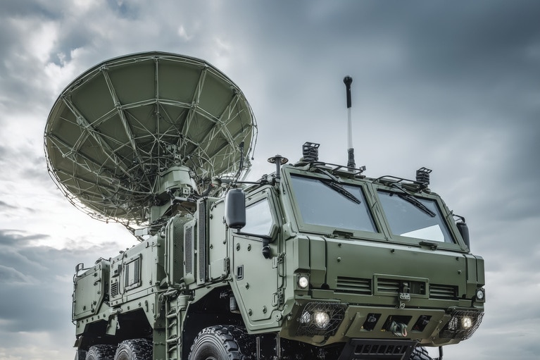
瞭解 Vicor 如何使用具有時間和高成本效益的 Vicor VPX 解決方案為地面移動雷達供電
高可靠性 VITA 62 電源,可滿足獨特電流要求
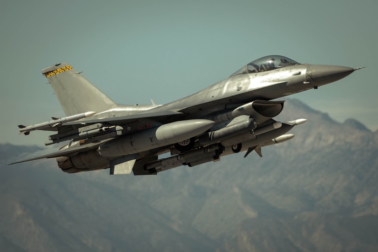
瞭解 Vicor 如何使用 Vicor VPX 產品的高功率和高電流傳輸為飛機雷達供電