48V 迁移之路上的 12 项技术挑战
为帮助您为迁移到 48V 做好更充分的准备,以下梳理了 12 项需要重点关注的挑战
要直观地说明电源时序的重要性,可以设想在一个大型工业系统中,如果其电机和执行器先于控制电子设备通电会发生什么情况。显然,必须通过精心设计的电源启动顺序来彻底消除此类不可预测且危险的隐患。同样,关机顺序也至关重要。
错误的电源时序不仅会在半导体器件层面,还会在系统层面引发问题。例如,这些问题可能导致 CMOS 器件出现意外的反向偏置,从而损坏或摧毁该器件,或将其锁定在只能通过重启电源才能解除的导通状态。尽管阻塞二极管可以防止闩锁效应,但会限制可用模拟输入电压的范围,因此采用电源电压启动时序是首选解决方案。此外,DSP、微处理器等多电压器件通常要求先提供 I/O 电压再施加内核电压。英特尔处理器芯片文档中通常会明确说明必须遵循的启动与关断顺序。同样,CPU 芯片必须在系统图形 IC 之前上电,以防止向图形显示器输出失控信号。
典型的电源时序方法有两种:一种基于电源,另一种基于逻辑。
“电源”解决方案利用某一电源轨的电压上升信号,向 N 沟道 MOSFET 发送一个适当延迟的触发信号,从而控制第二个电源轨的供电。“逻辑”解决方案则基于电源模块器件(power train device)的使能(Enable)引脚或其他逻辑引脚进行控制,而非直接控制其供电电源。利用电源组件内部集成的逻辑可实现成本更低、结构更紧凑且更简洁的解决方案,但在要求更高的应用中,MOSFET 能提供更精确的导通时间控制。
下图 1 展示了一个采用 N 沟道 MOSFET 和比较器的基础 MOSFET 时序电路。VREF 用于设置 VCC2 的切换阈值,VCC2 将在 VCC1 启动后经过 RC 网络设定的延迟时间才启动。MOSFET 驱动器内置一个电荷泵,确保 VGS 比 VCC2 高出数伏,从而完全增强 MOSFET 开关。该电路也确保 VCC2 会随 VCC1 关闭而关断,但由于 RC 网络的存在,VCC2 的关断会滞后于 VCC1。此外,如果 VCC1 无法用作参考电压,可能会出现其他问题。
图 1:采用 RC 网络、比较器和 MOSFET 驱动器的电源时序
图 1:采用 RC 网络、比较器和 MOSFET 驱动器的电源时序
目前已有集成度更高、更简便的解决方案,如图 2 所示的示例。
图 2:采用 MAX6819 的电源时序
图 2:采用 MAX6819 的电源时序
该时序器确保 MOSFET 始终获得所需的最小 VGS 增强电压,从而最大限度地减少 MOSFET 的损耗,并确保较低的漏源阻抗(RDS(ON))。MAX6819 预设了 200ms 的出厂固定延迟时间,该延迟发生在主电压超过设定阈值之后、启用电荷泵驱动外部 MOSFET 开关之前。
Vicor 稳压器、VI Chip 及砖型产品可通过上述 MOSFET 电路实现时序控制,也可如前所述通过其控制引脚和内部逻辑进行管理。一种简单的配置方式是,将某器件的“软启动”输出连接到另一器件的逻辑使能/禁用引脚,从而有效控制其电源时序。此外,许多 Vicor 器件都配备电压控制引脚或触发引脚。如果向该引脚施加斜坡电压,器件的输出将随电压控制输入呈斜坡变化,但会存在固定的时间延迟。
48V 迁移之路上的 12 项技术挑战
为帮助您为迁移到 48V 做好更充分的准备,以下梳理了 12 项需要重点关注的挑战
革新高压移动供电的电气化之路
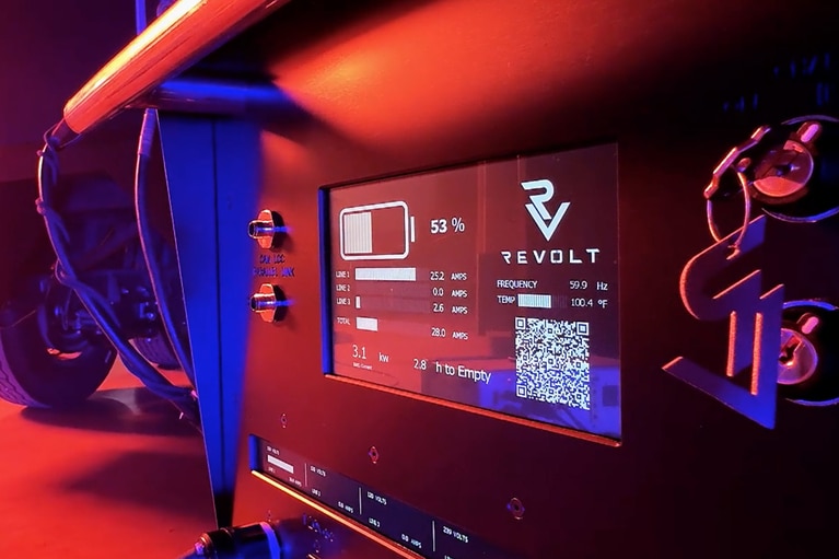
ReVolt 为电影片场注入活力!了解他们如何使用 Vicor 高密度电源模块取代柴油,实现清洁的移动供能
电源架构为何制约新太空 AI 任务
卫星 AI 的发展速度已经超越了传统电源系统。现代计算需要超低电压、大电流的供电能力,而传统电源架构直到现在都无法满足这一需求
AI 在太空赋能快速通信,开启创新新纪元
Spacechips 携手 Vicor 打造了 AI1 应答器,这是目前在轨运行中功率密度最高的处理器板。分比式电源架构可提供 133 TOPS 算力用于实时卫星自主运行和 130A 处理