

12 technical hurdles to negotiate on the road to 48V
To help you better prepare for your 48V migration consider the following 12 challenges
Learn how advanced high-current-density power modules and vertical power delivery methods can realize a significant improvement in processing performance, while reducing power losses, and saving terawatts of energy annually at the global scale.
By Maury Wood, Vice President of Strategic Marketing
Data centers consume a stunning amount of energy to power and cool generative artificial intelligence (genAI), compute and infrastructure hardware. The training of genAI artificial neural network models typically consumes months of time, with thousands of multi-billion transistor processors, high-bandwidth semiconductor and magnetic memories, and optical network processors operating perpetually [1], [2]. The New York Times has reported that “In a middle ground scenario, by 2027 AI servers could use between 85 to 134 terawatt hours (TWh) annually [3].” GenAI model training presents a daunting and pressing power consumption challenge which is misaligned with societal net zero and greenhouse gas reduction objectives.
This article discusses genAI processor power delivery options, and how advanced high current density power modules and vertical power delivery methods can realize a significant improvement in processing performance, while< reducing power losses, and saving terawatts of energy annually at the global scale.
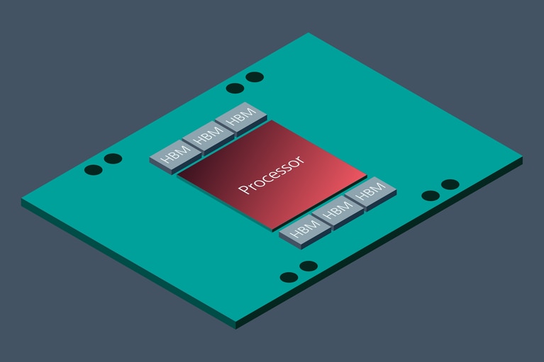
Over the past several years, numerous genAI processors targeted to large language model training have been introduced. The semiconductor process and packaging innovations embodied in these processors (Figure 1) is astounding, with >100 billion transistors fabricated in 4nm CMOS logic process technologies, and >144 gigabytes of high bandwidth memory (HBM) (another 1.128 trillion transistors) capable of >9.6 terabyte per second transfers [4]. The operating current demands of these processors are very significant and are now approaching 2000 amperes (A) peak, resulting in environmentally consequential levels of processor power loss and related thermal management complexity. Delivering 2000A at 0.7V utilizing voltage regulators at the point-of-load (PoL) presents a very interesting and important thermal and electrical performance challenge.
Today’s solutions use thirty or more voltage regulator (VR) modulated phases arranged laterally around the genAI training processor, adding wasteful I2R losses of 50 watts or more in the motherboard PCB copper power planes. One solution to this excess power loss and thermal management burden is to constrain the performance of the genAI training processor to a safe operating zone, leaving tera floating point operations per second (FLOPS) of performance on the table. A better solution is to move to vertically placed PoL power delivery, but this requires a major increase in component current density and new power module packaging technology.
Figure 1: GenAI training processors including high bandwidth memories (HBM) are mounted on accelerator module printed circuit boards.
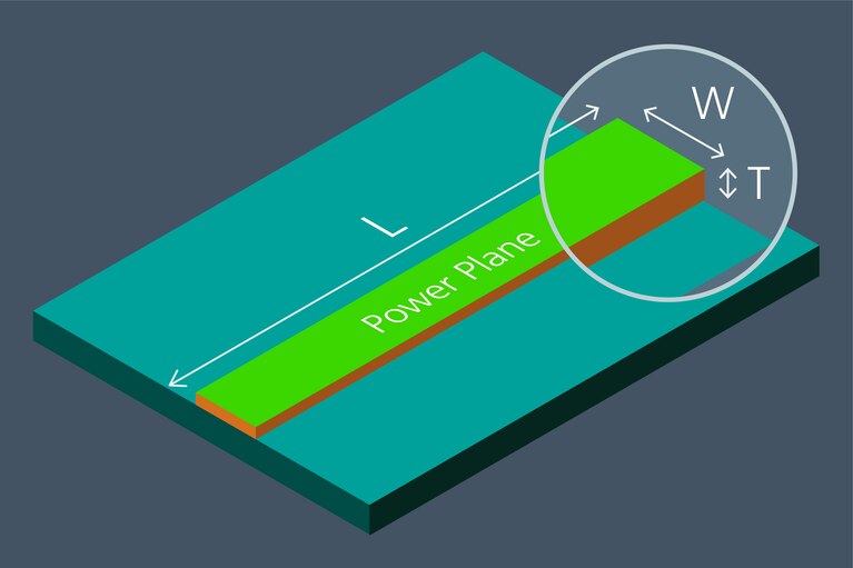
The printed circuit board (PCB) resistance is proportional to copper resistivity, power plane area and thickness, and temperature.
Copper PCB power plane resistance is conceptually modeled (Figure 2) by the equation:
R = [(ρ ⋅ L) / (T ⋅ W)] ⋅ [1 + α ⋅ (Celsius ambient temperature—25°C)]
Where:
ρ = copper resistivity (1.7 x 10⁻⁶ ohm-cm)
L = plane length (cm)
W = plane width (cm)
T = plane thickness (cm)
α = copper temperature coefficient (3.9 × 10⁻³/°C)
As can be observed in this equation, power plane resistance is linearly proportional to plane cross-sectional area [5]. By relocating the PoL converters closer to the genAI training processor, the power plane area and power delivery network (PDN) DC resistance can be reduced. GenAI processor power system designers increasingly recognize the critical
importance of PCB power plane area as an important means to reduce overall accelerator module (AM) power losses. As a result, they seek engineering improvements in current density and improved PoL VR power module packaging to enable placement closer to the
processor power pins.
Figure 2: Printed circuit board model.
GenAI training processor PoL power management is complex, with multiple power domains, including the main rail (core VDD) as low as 0.7 volts, only able to tolerate overshoot and undershoot of ±5% or so. Current draw is algorithm workload-driven (i.e., software task-dependent), which results in extremely high levels of time-rate-ofchange-of-current (dI/dt) of 2000A per microsecond or more. This high dynamic range requires the PoL power delivery solution to have a peak current capability (for 1 to 2ms duration typically) of about twice the continuous dc current level.
The HBMs in the processor array have their own voltage domain (HBM VDD) at 1.1V or 1.2V nominal, and also have constraints in terms of continuous and peak current requirements, dI/dt, and transient voltage limits above and below the nominal operating voltage to avoid circuit damage or operating life degradation. There are also auxiliary voltage domains (aux VDD) on the processor array with current requirements from roughly 250 to 400A.
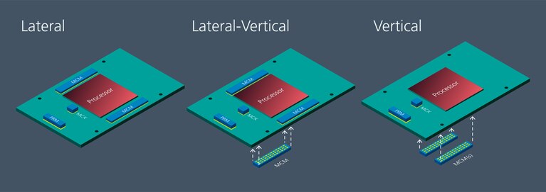
Figure 3 shows three power module placement options for VR power delivery, lateral (LPD), lateral-vertical (LVD) and vertical (VPD). Placing VRs directly under the processor, as with the LVD and VPD options, reduces the PDN resistance. This minimizes the power plane area with the advantages as discussed, but is typically where the large array of bypass capacitors are located, providing high bandwidth bypass and transient current supply for dynamic genAI workloads.
Figure 3: Power delivery network PoL placement options.
The decoupling capacitors needed to support a genAI training processor must be located as close as possible to the power and ground micro balls of the complex chipset package, and thus compete with the VRs for available PCB area. The bypass capacitance required relates to the processor rail’s power supply ripple tolerance, the voltage regulation subsystem frequency response, and several other factors [6].
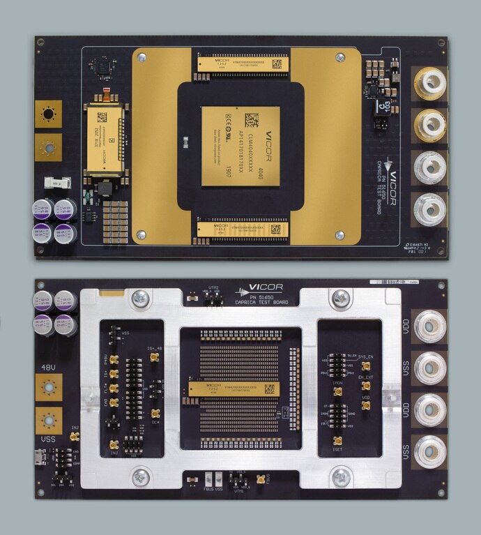
Unsurprisingly, a 1000A Thermal Design Current (TDC or continuous draw) genAI training processor requires a large amount of bypass capacitance, 3mF or more, which typically occupies the entire PCB area beneath the processor, leaving little room for VR placement within the capacitor component array. With a VR current density of 1A/mm2, which is the current state-of-the-art, it is just possible to fit a power module capable of 350A (continuous) in a 3500mm2 area among the bypass capacitors, and still achieve the requisite dI/dt performance. To evaluate the performance of this VR placement method, a test board (Figure 4) was developed to measure the thermal loss improvement LVD power delivery offers to a 1000A core VDD processor compared to a pure lateral module placement. The bottom side vertically-placed module shares the processor main rail current delivery duty with two other 350A (continuous) modules with the same footprint, which deliver power laterally on the top side of the board as shown in Figure 4.
Figure 4: Evaluation test board with lateral-vertical (LVD) power delivery.
The lateral-vertical layout approach was found to have significant advantages over a pure lateral design. One important note—the test board was designed with a load module and not an actual processor, where high-speed signal > routing (such as SERDES-based serial lanes) and other PCB design considerations would have to be taken into account.
Test results show that migration of one of the core VDD PoL power modules from lateral to vertical placement under the processor reduced the PDN impedance by a factor of six. The parallel lumped PDN impedance dropped from 60 to 11μΩ in aggregate for the three power modules used to supply the full 1000 continuous A, and the PCB dissipation dropped from 60 watts in lateral power delivery to 11 watts in lateral-vertical power delivery. This is a reduction of 50WPCB at 1000A load current per accelerator module, and 3200WPCB continuous for a genAI processor data center rack comprising 64 genAI AMs.
Using public domain demand forecasts of genAI accelerator modules in the coming years (more than 2.5M units in 2024) [8], [9], [10], and using reasonable forward-looking estimates of the cost of electrical power ($30 USD per megawatt-hour), this 50 watt savings per AM leads, by 2027, to terawatt-hours of power savings at the global data center level, equivalent to billions of dollars of electrical operating costs, plus millions of tons of carbon dioxide emission reductions (depending on the renewable energy mix) annually and in perpetuity.
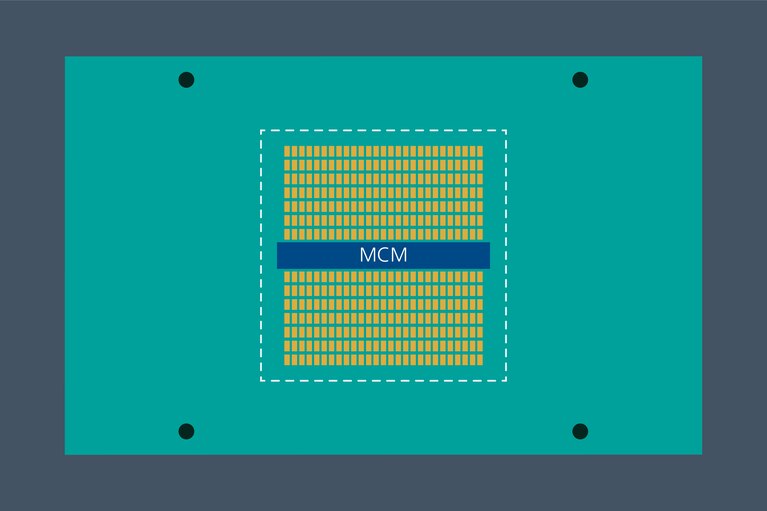
To achieve pure vertical delivery for the high current core power rails in this example would require an increase in VR current density by 3× or greater, from about 1A/mm2 to about 3A/mm2 (for a typical 3500mm2 training processor package footprint) to fit within the bypass capacitor array (Figure 5). Achieving this multiplicative step-up in current density demands a complete rethinking of the traditional VR approach, including the power module packaging.
Figure 5: Voltage regulator placed in the processor bypass capacitor array.
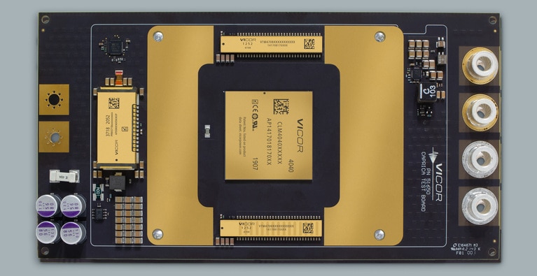
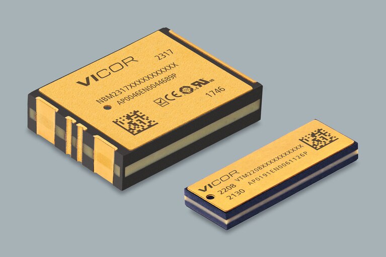
The general challenge with increasing the current density of PoL VRs is the size of the magnetic components needed for energy storage. Multi-phase VR and coupled inductor VR (Trans-Inductor Voltage Regulation or TLVR) architectures rely on energy storage in magnetic components (inductors or transformers respectively), and transferring the stored energy (as current) to the processor. Recently introduced power modules of this variety have modestly higher switching frequency and output current specifications, and are more compact, with two modulated phase stages per power module. These components generally regulate from 12VIN, fed by 48V fixed-ratio (K = 1/4) bus converters. Alternative approaches use lower voltage (typically 6VIN) lateral MOSFETs which are switched at somewhat higher frequencies, reducing the size of the energy storage inductors. These lower input voltage PoL VRs are fed by 48VIN to 6VOUT (K = 1/8) bus converters, which output much higher current levels, around 160A, unfavorably increasing the intermediate bus power losses in the PCB (WPCB). Due to physical limits on maximum switching frequency, even at 6V, traditional multi-phase and TLVR approaches achieve around 1A/mm2 current density maximum. Both topologies result in power modules that are tall (from 4 to 8mm) and relatively heavy, largely due to the magnetic (typically ferritic) energy storage components. Another early approach, introduced by Vicor in 2016, integrated the bypass capacitor array into a stacked power module as shown below (Figure 6). An additional “gearbox” layer mapped power to the processor ball grid array, making each device model a custom solution. This method has both scalability and cost challenges compared to a standard product family.
Figure 6: Module package for VPD with a stack-up that includes a gearbox layer.
Switching at significantly higher frequencies (greater than 1MHz) reduces the size of the energy storage components. However, for multi-phase buck or TVLR VRs, this approach necessitates reducing the operating voltage of the power MOSFET switches. The legacy fully integrated voltage regulator (FIVR) architecture is a classic example, where to avoid the bypass capacitor PCB density issue, onsilicon wafer buck regulators switching at MHz rates were able to achieve the current densities needed. Server CPUs at that time used an off-chip supply voltage of 1.8VEXT, and therefore a current gain of only 2× (1.8VEXT / 0.85 core VDD) resulted from the FIVR approach. Efficiency was reported to be in the 80% range.
For a 1000 to 2000A TDC genAI training processor, higher current gains and higher efficiencies are needed to avoid excessive thermal losses. In the 12 and 6 V VR architectures cited previously, current gains are in the 20× and 10× ranges, respectively (for a 0.7 V core VDD processor).
But with the 30 or more modulated phases needed for the core rail, these architectures do not achieve the required 3A/mm2 current density to allow VR placement embedded within the bypass capacitor array field.
Power modules that use transformer-based current multiplication instead of traditional voltage averaging have the advantage of higher current multiplier gains, in the 48 to 60× range. This topology has inherently lower switch operating voltages, for example, with 48× factor current multiplication (K = 48/1), low voltage power switches can be used at the PoL. These modules are operated above 1MHz with efficiencies in the 94% range, due to zero-voltage switching (ZVS), zero-current switching (ZCS), and zero energy storage techniques. Magnetic components are used for the transformation of voltage and current only, and are not utilized for magnetic energy storage. With high switching frequencies, the modules can be made remarkably small. With new 3Di power module packaging, the requisite current density of 3A/mm2 for pure VPD on the core VDD rail can be achieved, and further advances in current density are possible in the future.
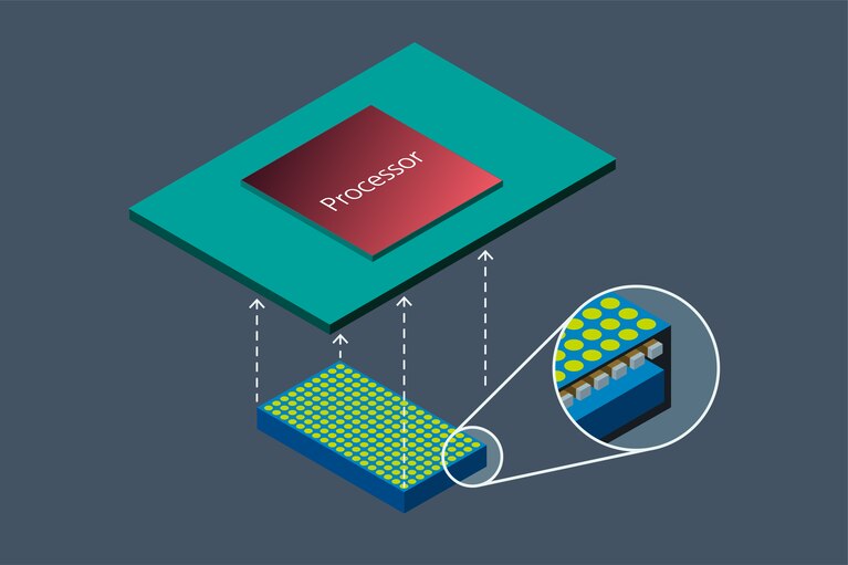
Advances in power module packaging to enable VPD must also be conducive to high-volume contract manufacturing environments. The module package (Figure 7) must be thermally adept to simplify the heat management solution for VPD. Advances in material science and magnetics with greater than 1MHz switching frequencies have enabled 3Di technologies, resulting in very thin (<1.8mm) packages with very low thermal resistance and favorable surface-mount capabilities. The 3Di packages are mechanically rigid, have a high degree of co-planarity, and the 3Di package plating helps to mitigate radiated electromagnetic interference (EMI).
Figure 7: Example overmolded, 3D interconnect power modules.
As future genAI training processors become more complex, with stacked die and multi-processor chip arrays in a single package, continuous operating current levels are hurtling towards 2000A and 1500 watts or more. Exascale genAI supercomputers running multi-trillion parameter large language models will continue to use thousands of AI and CPU processors per system [11]. This application will, without doubt, remain the most power-intensive and thermally-challenging in the modern computing world for the foreseeable future. Suppliers to the genAI component ecosystem are ethically obliged to help mitigate the power consumption of this amazing new technology.
[1] (2024). Real-Time Trillion Parameter Model NVIDIA GB200 NVL72. [Online]. Available: https://www.nvidia.com/en-us/data-center/gb200-nvl72/
[2] (Mar. 2024). Nvidia’s New Blackwell GPU Can Train AI Models/ With Trillions of Parameters by Agam Shah, HPC Wire. [Online]. Available: https://www.hpcwire.com/2024/03/18/nvidias-new-blackwell- gpu-can-train-ai-models-with-trillions-of-parameters/?utm_ source=HPCwire+Newsletter&utm_medium=email&utm_campaign=&utm term=5245H9859712A5Y&oly_enc_id=5245H9859712A5Y
[3] (Oct. 10, 2023). A.I. Could Soon Need as Much Electricity as an Entire Country. The New York Times Newsletter [Online]. Available: https://www.nytimes.com/2023/10/10/climate/ai-could-soon-need-as-much-electricity-as-an-entire-country.html
[4] (Mar. 22, 2022). NVIDIA Hopper Architecture In-Depth by By Michael Andersch, Greg Palmer, Ronny Krashinsky, Nick Stam, Vishal Mehta, Gonzalo Brito and Sridhar Ramaswamy, Technical Blog, NVIDIA Developer. [Online]. Available: https://developer.nvidia.com/blog/nvidia-hopper-architecture-in-depth/
[5] (2021). Trace Resistance Calculator, All About Circuits. [Online]. Available: https://www.allaboutcircuits.com/tools/trace-resistance-calculator/
[6] (Dec. 5, 2006). Power Bypass Decoupling of SHARC Processors by Larry Hurst and Alberto Comaschi, Engineer-to-Engineer Note (EE-253), Analog Devices. [Online]. Available: https://www.analog.com/media/en/technical-documentation/application-notes/ee-253.pdf
[7] (2022). Intel Pentium Silver and Intel Celeron Processors Datasheet. [Online]. Available: https://edc.intel.com/content/www/us/en/design/ipla/software-development-platforms/servers/platforms/intel-pentium-silver-and-intel-celeron-processors-datasheet-volume-1-of-2/005/fully-integrated-voltage-regulator-fivr/
[8] (Oct. 2023). AI Chipsets for Cloud and Datacenter Forecast Reprot, OMDIA Analyst. [Online]. Available: https://omdia.tech.informa.com/om015986/ai-chipsets-for-cloud-and-datacenter-forecast-report--analysis
[9] (May 2022). Checking Out the NVIDIA H100 in Our First Look by Patrick Kennedy, STH. [Online]. Available: https://www.servethehome.com/checking-out-the-nvidia-h100-in-our-first-look-at-hopper/
[10] (Aug. 2023). Nvidia H100: Are 550,000 GPUs Enough for This Year? by Doug Eadline, HPC Wire. [Online]. Available: https://www.hpcwire.com/2023/08/17/nvidia-h100-are-550000-gpus-enough-for-this-year/#:~:text=TheflagshipH100%20GPU(14%2C592,basedsupercomputercalledShaheenIII
[11] (2024). AI Index Report, Standford University. [Online]. Available: https://aiindex.stanford.edu/report/
This article was originally published by IEEE.
Maury Wood is Vice President of Strategic Marketing at Vicor Corporation. Prior to joining Vicor, Maury held senior roles at optical fiber test and semiconductor companies, including EXFO, AFL, Broadcom, NXP, Analog Devices, Cypress, Mercury and BAE. He hold a BSEE (Electrical and Computer Engineering) from the University of Michigan, and did graduate studies at Northeastern University, Babson College, and MIT. He enjoys climbing, backcountry skiing, mountain biking, and playing jazz bass.
Maury Wood, Vice President of Strategic Marketing
12 technical hurdles to negotiate on the road to 48V
To help you better prepare for your 48V migration consider the following 12 challenges
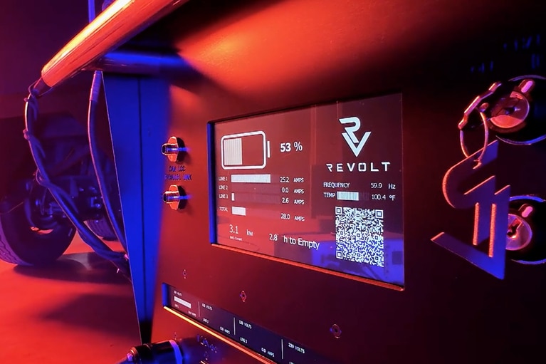
Innovating the electrification of high-voltage mobile power delivery
ReVolt is electrifying film sets! See how they use Vicor high-density power modules to swap diesel for clean, mobile energy
Why power architectures constrain New Space AI missions
Satellite AI outpaces legacy power systems. Modern compute needs sub-volt, high-amp power that traditional architectures simply can't deliver until now
Harnessing AI in space to enable faster communication and a new era of innovation
Spacechips & Vicor created the AI1 Transponder, the densest orbital AI board. FPA enables 133 TOPS for real-time satellite autonomy and 130A processing