
Digitimes key pathways for unmanned vehicle technology
Learn about high-density power conversion for UAVs
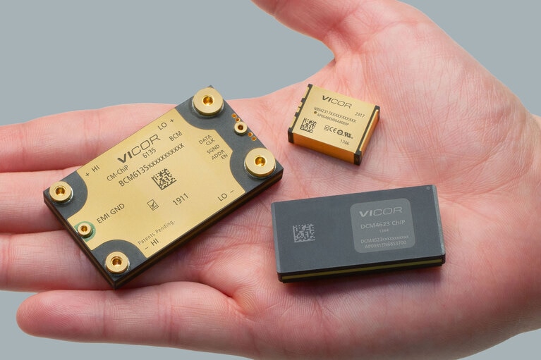
A few rules of thumb help navigate the nuances and common pitfalls of power system design using power modules.
By Jeff Ham, Principal Applications Engineer
With industry emphasis on minimizing and eliminating waste wherever possible, it is the responsibility of the system designer to optimize the overall power architecture. Every piece of electronic equipment has a power delivery network (PDN) typically comprised of, but not limited to, cables, bus bars, connectors, circuit board copper power planes, AC-DC and DC-DC converters and regulators. Everything within this network influences how well the design functions as it sees line, load and environmental variations.
Historically, power architectures have been defined in the late stages of product development, when space and options are already limited. A more proactive approach that places architecture design early in the process lends itself to producing more robust systems able to accommodate changing design specifications during development.
Power designers often focus on the conversion stages to maximize conversion efficiency and minimize power loss. The primary driver has been thermal management because the conversion stages are typically among the largest contributors to the thermal load. High power dissipation requires more complex and extensive cooling methods which all add cost and size, especially for applications in harsh environments.
Dissipated power is the difference between input power and output power. One determines the power converter’s dissipated power by dividing the power rating of the converter by its decimal equivalent efficiency: A 100-W-rated converter with an efficiency of 80% will have in input power of 125W and a dissipated power of 25W. It is critical to consider each element in the system this way to determine total system losses. Boosting efficiency by even a small amount can significantly reduce losses. For example, a 10-point rise in efficiency–to 90% in this example–may not seem like much, but it reduces the power dissipated by more than half: 11.1W down from 25W.
What does this efficiency increase do for the power delivery network? Apart from reducing the thermal impact of a converter, it also reduces the demand on the input source which needs to deliver less power. This lower power use also means that for a given input voltage, the source current is also lower. From Ohm’s law, power can be viewed as the product of voltage and current and as the product of resistance and the square of the current (P = VI = I2R). In analysis of power delivery networks it is the resistance term that is frequently overlooked. All paths from the source to the load have a fixed resistance. All of them bear on the power loss in the aggregate system. There are also safety and stability components that contribute to overall power loss that must be accounted for: fuses, circuit breakers and filters for electromagnetic interference reduction and voltage smoothing. In each of these elements, there is a voltage drop penalty that can degrade the stability of switching regulators and create other issues within the system.
End-use equipment (that the power delivery network supplies) that has large power swings like a CPU, pulsed load, or motor will cause significant voltage variation at the converter input and output. As a general rule of thumb, the source impedance the converter sees should be a factor of ten less than the lowest impedance the converter presents.
Going back to the 90% efficient 100-W converter example, let’s say the operational input range for this device is 18 – 36V. At an input of 18V the converter draws about 6.2A. The converter input impedance (R) is therefore V/I or 18/6.2 = 2.9Ω. At 36V the input current is half, so the impedance is 11.7Ω. At the converter’s lowest input impedance, the rule of thumb dictates that the source impedance to assure stable operation should be no more than 0.29Ω.

Figure 1: A 12-V low-voltage PDN supplying five independent loads. In this example the loads are low voltage (< 5VDC) and have higher current flowing between them and the converters (shown by the thick trace).
A point to note is that system stability is important when designing a power system. This simplistic resistance discussion does not account for the reactive elements, e.g., capacitance and inductance, both real and apparent in place which can cause resonances and other problems if not well understood. These topics are beyond the scope of this article.
What can be done to optimize the PDN as it relates to system power loss?
Whether it is analyzing an existing design or creating a new architecture from scratch, the approach is the same.

Figure 2: An Improved PDN with the source voltage raised from 12 to 48VDC. The five independent loads have the same current requirements as those shown in the first example. As a result of the higher source voltage, the current flowing from the battery to the conversion stage is lower (indicated by the thin trace).
First: Though it may sound obvious, use the most efficient available converters. Consider the PDN in two parts: the outputs from the actual application load(s) to the first conversion stage including any intermediate conversion stages, and the input from the source to the first conversion stage.
The application load will have a predetermined minimum voltage requirement. The current demands for modern electronic systems can be high, in some cases exceeding 1,000A at sub-1-V levels. To minimize losses in these applications, point-of-load (PoL) converters are placed near the load consuming the power.
PoL avoids long wiring distances between the converter and load characterizing conventional power supplies and provides a precise voltage supply that meets low-voltage/high-current needs. The PoL stage should be located as close as physically possible to the load it powers to minimize the interconnect resistance.
Moving toward the input, the PoL input voltage should be as high as practical. Consider a 12-V low-voltage PDN supplying five independent loads. In this example the loads are low voltage (< 5VDC) and have higher current flowing between them and the converters.
Such a setup could be a legacy computer supply, vehicle power system or drone payload. There is a fixed trace resistance to the input to the PoLs that will have a given power dissipation for any given operating power level. If we can increase the voltage by a factor of four (i.e., to 48V) at the same power, the current flowing in this leg is now one-quarter of the previous level. Thanks to the squared current term in the power equation, the new power dissipation is significantly less, and there is a reduction in voltage deviation too.
Additionally, 48V is a good distribution voltage because it is also within Safety Extra Low Voltage (SELV) limits, defined by the IEC as having a low risk of electrical shock. For an existing application, raising the voltage will require different PoLs. Here, a modular approach using a device having the same package size will be an easy conversion because the converters will be drop-in replacements.
Example: Tethered-UAV power delivery network


Figure 3: Top, comparison of current, voltage drop and power loss reduction for different source voltages in each tether conductor for the airborne vehicle requiring 500W. Below, optimized tethered drone PDN from the ground supply to the airborne vehicle. The 800V used within the tether minimizes the critical transmission losses and voltage variations due to the operation of the UAV. Because the current is significantly lower than with lower supply voltages, the move to 800V has the added benefit of potentially reducing the tether windage and weight by allowing for the use of smaller-gauge conductors.
Consider the more extreme example of a tethered UAV or drone and specifically, the effects of the source-to-first conversion stage. The tether represents the interface between the ground supply.
Assume the UAV tether is 100 ft long and contains 24-AWG conductors, each of them having approximately 2.5 Ω of resistance per 100 ft.At a 48-V distribution, the current in this tether is about 10 A; the resistance is 5 Ω for the 100-foot round trip, so the power lost in the tether is 500 W! Clearly this UAV can’t fly because the tether dissipates all the power, leaving nothing for the vehicle.
Now consider use of a higher input voltage. Assume a 400-V system with the same conditions as above.
At a 400-V distribution, tether current drops to about 1.25 A and the tether only dissipates about 8 W. Doubling the input to 800 V drops the tether current to about 0.6 A, reducing power dissipation in the tether to about 2 W. The lower current draw potentially makes possible the use of smaller-gauge tether conductors, potentially reducing drag and windage and possibly the power needs of the UAV as well.
Power dissipation is one thing, but regulation at the end of the tether is also important. The regulators onboard the UAV will have a defined input voltage range. There is a voltage drop across the tether resistance. Given the 24-AWG 100-ft tether and its 5-Ω round trip resistance, there is a 5-V drop for every amp of current. Reducing the voltage dropped across the tether also reduces the ratio of the voltage drop over applied voltage, further improving regulation: If the voltage doubles and the current is halved, the the drop across the tether halves and the ratio of tether drop to load voltage is quartered.
It should be apparent moving to an 800-V source for the ground supply is the way to optimize power transmission up the tether. But the UAV must convert that 800 V down to low voltages to power its motors and electronics. For this part of the PDN, 48 V for the onboard electronics makes the most sense for reasons described earlier.
All in all, the path to optimize a PDN can be summarized into six steps:
This article was originally published by Power Electronic Tips.
Jeff has been with Vicor for 25 years – and been in the power industry for 39. He holds a BSEE from Northeastern University.
His email address is jham@vicr.com.
Jeff Ham, Principal Applications Engineer
Digitimes key pathways for unmanned vehicle technology
Learn about high-density power conversion for UAVs
Accelerate your move to a high performance 48V power delivery network
This eBook provides guidance on designing 48V power delivery networks to enhance the performance, efficiency, and reliability of industrial products
Build better UAVs using modular power
Power Delivery Networks (PDN) based on Vicor high performance power modules enable innovative designs for the next generation of UAV development
UAV Market Trends and Power System Seminar 2025 Taipei, Taiwan
Power modules enable top performance and innovation for today’s advanced UAVs