by Tom Curatolo, Principal Technical Sales Engineer
A system’s power delivery network or PDN is made up of passive and active components such as cables, connectors, AC-DC and DC-DC converters and regulators. As power levels increase to enable new features and the electrification of mechanical and hydraulic systems, PDN performance is becoming more critical, and in some cases, constraining end system capabilities because of PDN footprint, weight and power losses.
Power system design engineers are under increasing pressure to design a PDN that is small, lightweight and highly efficient, as this achievement can define a leadership product capable of delivering major end-system performance and competitive advantages for OEMs.
Forty years of innovation
Understanding the importance of these power system design challenges and key PDN performance specifications drives Vicor to constantly innovate to stay on the forefront of power systems technology. To do so requires a major commitment to innovation on many levels.
Four pillars of power innovation:
- Power delivery architectures
- Power conversion topologies
- Control systems
- Power module packaging
Each level has multiple dimensions, and each depends on the others. Together, the four levels of power innovation advance power module performance. Architecting the PDN is the first step for any power systems engineer and a great architecture can ultimately define overall performance.
Architecture development involves asking questions critical to optimizing performance: When to convert, regulate and isolate? What voltages will be used and distributed within the PDN?
Answers will vary according to need, but the modular elements of the solution are the same, leveraging high-frequency switching (power conversion) topologies enable reductions in passive and magnetic component values and hence their size, while innovative control systems such as zero-voltage and zero-current switching can significantly reduce power losses.
Advanced materials for circuit boards, magnetics, semiconductors and passives enable reduced power losses and component sizes.
However, all of this would have little impact if not for the constant innovation of power module packaging, which ultimately defines the power and current density.
Power module packaging is a unique differentiator for Vicor and has been a core competency since the company’s inception. In 1984, the modular Brick DC-DC converter component, so called due to its form factor, was introduced with innovative attributes:
- Enabled a distributed power architecture
- High-efficiency quasi-resonant forward converter topology
- A frequency-modulation (FM) control system with zero-current switching (ZCS) to reduce power loss
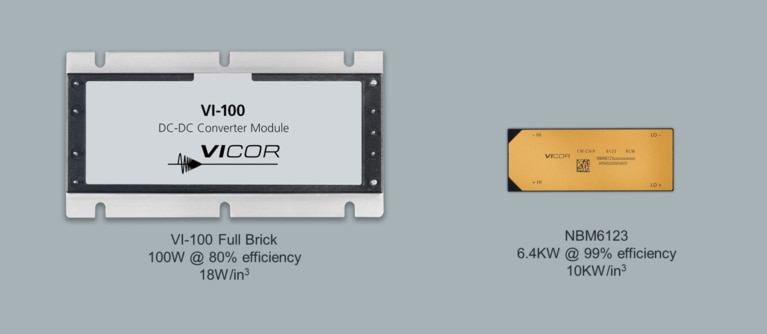
With switching frequencies as high as 1MHz, the physical size of the passive components and magnetics was significantly decreased, and the reduced power losses enabled a power module with breakthrough power density, which changed the power supply industry (Figure 1).
Figure 1: From the early Brick which offered leadership density and efficiency to today’s ChiP, Vicor has driven significant advances for power systems engineers, particularly in the area of power density.
Turning the corner from Bricks to VIChip and ChiP packaging
In 2008 Vicor introduced new innovations which enabled significant gains in power density over the Brick and advanced its power component design methodology for the power systems industry (Figure 2):
- The Factorized Power Architecture (FPA™)
- A new higher-frequency topology called a Sine Amplitude Converter (SAC™)
- Zero-voltage switching (ZVS) and zero-current switching (ZVC)
- New packaging materials
The new architecture, combined with the higher-frequency switching topology and control system ZVS and ZCS improvements, once again reduced power losses and enabled higher levels of power module integration that drove a new package development, the VI Chip. The package was a fully overmolded PCB assembly using a thermally-effcient molding compound incorporating specialized materials developed in conjuction with key suppliers. The module was manufactured in individual mold cavities and incorporated J-lead pins for surface-mounting on customer’s motherboards. The resulting family of new power modules offered breakthrough performance in powering sub-1V highcurrent processors developed by IBM for its supercomputers and set the stage for Vicor 48V-to-load leadership in the data center and AI processor markets a decade later.
Figure 2: VI Chip and ChiP packaging was necessary to fully realize the breakthrough advances of the new Factorized Power Architecture and continual advances in topologies, control systems, components and materials.
In 2015 further improvements in control systems, topologies, components and materials enabled the redesign of the VIChip® package to capitalize on further power-loss reductions, higher-frequency control systems and topologies with resulting gains in power and current density. The new package was called the ChiP™ (Converter housed in Package), and its construction and manufacturing approach broke new ground at Vicor as well as in the power module manufacturing industry. The new ChiP package was distinguished by its two-sided component assembly while being cut from fixed-size panels, similar to how silicon chips are made and cut from wafers.
Key power module packaging attributes
While the four pillars of innovation have driven Vicor advancements, power module packaging most acutely distinguishes the company’s expertise. There are five attributes that make a converter or regulator module package truly world-class, enabling high-performance power delivery (Figure 3):
- High power and current density
- Thermal adeptness
- Integrated magnetics
- Compatibility with high-volume PCB assembly techniques
- Module production using high-volume automated manufacturing techniques
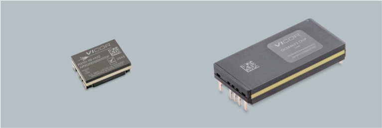
Each step of the power module package development leveraged new materials, active and passive components and, most notably, improvements in magnetic structures based on higher switching frequencies. The higher frequencies are enabled by topology and control system improvements incorporated in proprietary Vicor control ASICs. The recent launch of the fourth generation of these ASICs has enabled power density and current density numbers of 10kW/in3 and 2A/mm2 respectively, enabling a new family of AC and DC high-power front-end converters and point-of-load (PoL) current multipliers. These latest generations of modular power solutions are changing the way PDNs are architected and designed in both data center and automotive applications.
The multi-layer circuit boards within the power module are complex designs. They require special materials for optimal thermal conduction and to manage high currents and high voltages in minimal space, all while minimizing power loss.
Double-sided component placement enables heat extraction from both sides to maximize performance and power ratings. The copper-plated ChiP has further advanced ChiP packaging, significantly simplifying thermal management by means of a wrap-around copper jacket.
Materials science plays a big role in advancing power package performance, especially when switching at multiple-MHz levels.
The main energy storage core plays a critical role in overall module performance and can be one of the main sources of power loss in a power-system design. The core, its windings and PCB material compositions are continually optimized for higher switching frequencies, higher power levels and lower output resistances (ROUT) to reduce power losses as current levels for a single module rise into the hundreds of Amps. By integrating the energy storage inductor or transformer into a power module and maximizing its performance, the power-system designer is relieved of the often difficult and time-consuming process of optimizing an external inductor and can also reduce the overall power system footprint.
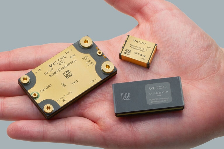
One power module family that captures all of these critical design elements is the current multiplier which is now powering some of the most advanced artificial intelligence (AI) processors used in highperformance computing applications. Vicor VTMs and MCMs are capable of delivering up to 1000A, while directly converting 48V to sub-1V levels. The integrated planar magnetics in these devices have been optimized over 12 years and now achieve current density levels of 2A/mm, with even further advances planned.
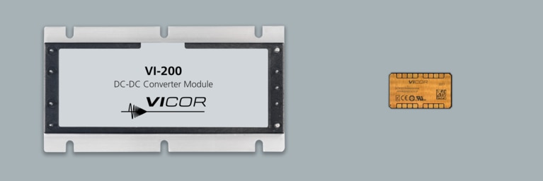
Figure 3: Advancements in topologies, control systems and new power delivery architectures has driven better power density for the past years and has shown a reduction in power losses of 25 % every 2.5 years, as shown by the early full-brick VI-200 DC-DC converter (left) and the latest stacked CHiP GCM and DCM modules (right).
Compatibility with high-volume PCB assembly techniques
Surface-mount reflow soldering is used by all of the high-volume contract manufacturers (CMs) around the world. The new SM-ChiP™ is a plated, overmolded package intended for surface-mount attachment to a printed circuit board and is compatible with CM manufacturing techniques and equipment. The electrical and thermal connections of the package are formed through soldered connections to plated castellation terminal features along the perimeter of the module and continuous plated surfaces of the main package body.
Module production using high-volume automated manufacturing techniques
ChiPs are made and cut from a standard-size panel and make full use of both sides of the modules’ internal PCB for active and passive components (Figure 4). Making and cutting ChiPs from panels is very similar the way Silicon chips are made and cut from wafers, enabling a manufacturing operation that is streamlined, high-volume and very scalable.
Figure 4: The new panel manufacturing process was another innovation for the power industry. ChiPs are all cut from the same size panel, enabling an automated high-volume manufacturing process.
Three-dimensional ChiPs enable AI and high-performance computing
More recent innovations in ChiP packaging are enabling several new high-growth applications. One of the most demanding is advanced artificial intelligence, where processor current levels have risen above 1000 amps. In these applications, power distribution loss in PCB copper power planes has become a dominant loss term and constrains performance.
To meet the requirements of these demanding applications, the best location for the power module to minimize impedances is directly under the processor and exactly matching the power modules’ output power pins withthe power pin array of the processor above. Unfortunately, this is also the optimal location for the large number of bypass capacitors required for energy storage to meet instantaneous processor power demands, creating a board layout conflict.
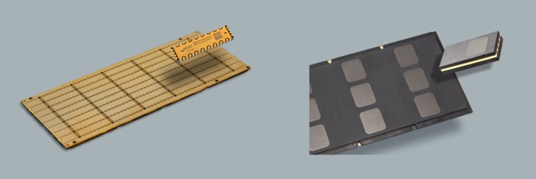
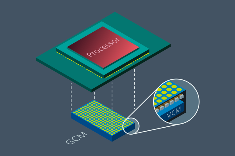
ChiP stacking for vertical power delivery
The challenge of vertical power delivery (VPD) has been met with a multilayer stacking technology (Figure 5). The new VPD power module consists of a current multiplier layer and a “gearbox” layer, which holds the bypass capacitors and changes the pitch of the current multiplier to match the pitch and layout of the AI processor power pin map above. This new multilayer packaging technology enables AI processor power system designers to deliver power in the most optimal way and to get the maximum performance out of their processor for high-performance computing (HPC) applications.
Figure 5: Vertical power delivery to advanced AI processors with stacked ChiPs reduces board and substrate power losses to improve processor performance.
Conclusion
The ChiP packaging approach focuses on the miniaturization of every single component and element that makes up the module. As Vicor makes further improvements in performance, ChiP packaging will exhibit new levels of innovation. For 40 years Vicor has pushed the limits of magnetics and power engineering routinely delivering the next generation of power-dense products for customer’s world-changing innovations. With this momentum and using the five pillars as a compass, the journey is nowhere near over.
Tom Curatolo is a Principal Technical Sales Engineer supporting the Aerospace and Defense sector. Tom has more than 40 years of experience in the high-tech electronics industry with specific expertise in power electronics and power architectures. He has been with Vicor Corporation for more than 30 years. The majority of his time with Vicor has been in Applications Engineering where he has extensive experience in supporting the diverse customer base and markets that Vicor products address. Tom received a B.S. degree in Electrical Engineering from Worcester Polytechnic Institute in 1985. Tom is based in Andover, Massachusetts.
Tom Curatolo, Principal Technical Sales Engineer