
Innovating power delivery networks
Vicor is innovating with power delivery networks. Improving end-system performance requires innovative power technologies
There are many articles available describing how to overcome power distribution losses with suitable power conversion devices and architectures. This post goes back to basics: explaining the underlying issues of distribution losses and the principles of their solution.
If DC-DC converters and power conversion devices are any part of your working life, you will be aware of their key role in conducting electrical power from the edge of a printed circuit board (PCB) to its onboard components efficiently. You may also be aware of the Vicor Intermediate Bus Architecture (IBA) and Factorized Power Architecture and other technologies designed to maximize this efficiency. The objective is to minimize distribution losses as the power flows from the PCB connector to its onboard point of load.
However you may not be aware of the fundamentals – what causes distribution losses, why does advancing technology exacerbate their impact, and how do power devices and architectures work to mitigate this? We provide answers to these questions below as we explain the underlying problems that FPA and other power architectures are designed to solve.
Even with mitigating technologies, distribution losses – or, more definitively as we shall see, I2R losses – are an inevitable part of transmitting power from one place to another. This is equally true of mains power transmitted across the National Grid or of low voltage DC power applied to a PCB. The reason is that the conducting medium, whether it is an overhead cable or a PCB track, always has a finite resistance, and power is lost, or dissipated, in overcoming this resistance. The remaining power is dissipated by the device being supplied; a microprocessor chip, for example.
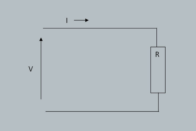
To understand more about the nature of electrical power dissipation, let’s start with Figure 1:
Fig. 1: Voltage applied across a load
Fig. 1: Voltage applied across a load
In Figure 1, a DC voltage (V) volts is being applied across a resistive load (R) ohms. The load is drawing a current (I) amps. At this point, we need to introduce a couple of formulae; however they’re the only two we have to understand. We can derive everything else from them.
Firstly, there’s Ohm’s Law, which says

Where V is the voltage applied across (say) a device, R is its resistance, and I is the current it draws. For a fixed voltage supply, we can see that the lower the device’s resistance, the more current it draws.
The other formula is Watt’s Law which states
This says that in Figure 1, the power (P) dissipated by the device is the product of the voltage (V) across it and the current (I) that it draws. Note that P depends equally on V and I. Note also that if a device takes, say, 100W, this could be delivered either as 100V @1A, or 1V @100A, or any other VI combination that multiplies out to 100. However in considering these variations we must not forget the device’s maximum input voltage rating.
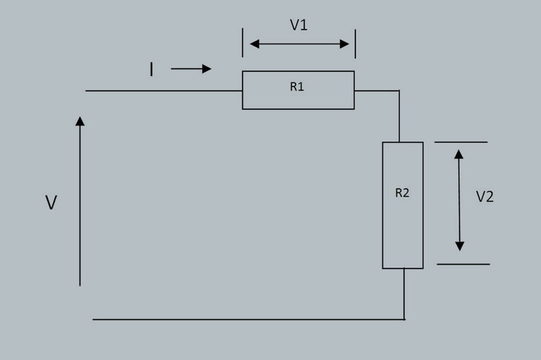
At this point, let’s imagine that the device in Figure 1 is a microprocessor, and that it draws 100A @1V. These are not real figures, but they are representative of what could be expected from a desktop PC chip. From Ohm’s law we can see that it has an internal resistance of V/I = 1/100 = 0.01 Ohm. As we move from Figure 1 towards reality – but without yet giving ourselves the benefit of modern power train technology – we recognise that the chip’s 1V supply has to travel along copper tracks connecting the board’s power connector to the chip’s power pins. These copper tracks have a finite resistance. If they are 5mm wide and 5cm long this could be approximately 0.005 Ohms. Note that the track resistance is directly proportional to the track length. Figure 2 represents the electrical view of this scenario.
Fig. 2: Microprocessor load on a PCB
Fig. 2: Microprocessor load on a PCB
In Figure 2, R1 represents the PCB track resistance of 0.005 Ohms while R2 represents the microprocessor internal resistance of 0.01 Ohms. Accordingly, if we now apply 1V to the board edge connector, Ohm’s law shows that the current would be:

not the 100A the chip may require. It also shows that there would be a voltage drop across the track of 66.7 x 0.005 = 0.33V – leaving only 0.67V across the chip. Track resistance has deprived the chip of both voltage and current.
Consider also the power lost through dissipation in the track. If P = IV and V = IR, then by substituting for V we can see that P = I2R. So, the power dissipated in track resistance R1 is 66.72 x 0.005 = 22W. In this case the distribution loss, or I2R Loss, is 22W.
These losses and inefficiency are clearly unacceptable, so what can we do? To see the answer, let’s suppose that our microprocessor is a very flexible or even magical device that can work on a 50V input supply just as well as on 1V. We know that it draws 100A at 1V, so according to Watt’s Law it consumes 100W. Therefore it will require 2A @50V. Importantly, in this new scenario, the device’s internal resistance would have increased from 0.01 Ohm to 50/2 = 25 Ohm.
So if we apply 50V across the connector in Figure 2, the actual current will be:

a very small loss in current to the device. The voltage drop across the track is just 1.996 x 0.005 or 0.0099V. The chip is enjoying nearly all of the available voltage and current. The dissipation across the track is 0.02W. By transmitting power at a higher voltage and lower current, we have delivered it where it is needed, with minimal transmission losses.
All of this prompts the question: If higher voltage levels are so beneficial for power transfer efficiency, why don’t chip makers produce devices with higher input voltages? The answer is that the manufacturers are driven by their own priorities, which are to deliver ever more processing performance while curbing the associated increase in power demand. Reducing the chip’s supply voltage contributes to both these objectives. So, over the years we have seen chips demanding steadily increasing current at steadily reducing voltages; a formula for increasing distribution losses! Pressure on power system designers to find a way of supplying the chip efficiently has grown accordingly.
An obvious solution would be to place a DC-DC converter physically close to the microprocessor chip. This can receive power at a high voltage and low current and convert it into low voltage and high current suitable for the chip. I2R losses are minimized because the track length and resistance between the converter and chip are minimized. In fact, one of the earliest responses was to use exactly this approach. However, continued development in electronic device and PCB design rendered it increasingly unsatisfactory. In reality, DC-DC converters had to handle isolation and voltage regulation as well as conversion, and their own size and electrical efficiency became increasingly important issues. This was especially true as the number of devices on a PCB, and the supply voltages they demanded, proliferated steadily.
For these reasons, more advanced approaches such as Intermediate Bus Architecture (IBA) and Factorized Power Architecture (FPA) as previously mentioned, have appeared. They are sophisticated tools that tackle these complex issues, yet the fundamental, underlying problem they solve remains the same: How to deliver increasing levels of power to increasing numbers of ever lower voltage devices, while minimizing distribution I2R losses en route to the point of load.
Product overview: Intermediate Bus Architecture (IBA)
Industries and innovations: Factorized Power Architecture (FPA)
Innovating power delivery networks
Vicor is innovating with power delivery networks. Improving end-system performance requires innovative power technologies
Build small, lighter power systems by eliminating bulk capacitance
Vicor's Factorized Power Architecture™ (FPA) delivers significant reductions in both size and weight
High efficiency converters help maximize run-time for autonomous warehouse robots
High efficiency converters help maximize run-time
Modular DC-DC system design done right
You will learn topics such as input and output filtering, protections, compatibility with the source and load dynamics

